IMS-Materials – Properties and Functions
The increasing technical requirements of the electronic industry regarding electrical and electronical devices partially result in thermal problems. Higher frequencies, smaller structures as well higher performance of the devices lead to considerably higher temperatures. In order to grant solid performance, a high degree of stability and a long life-cycle of the devices, it is necessary to control and dissipate the heat.
Why is thermal Management in PCBs necessary?
Why is thermal Management in PCBs necessary?
Nowadays, it is frequently necessary to dissipate heat from electronic modules in order to increase the life-cycle and improve the functionalities of modern modules. This is where the IMS technology comes in.
Main Application Areas for IMS Materials
Main Application Areas for IMS Materials
- Automotive electronics: e.g. braking and power steering, LED lighting
- Power electronics: DC power supplies, inverters, motor drivers
- LED technologies: e.g. displays, railway station lighting, illuminated signs
Ways of Heat Dissipation
Ways of Heat Dissipation
Heat can be dissipated in different ways, for example by:
- Radiation
- Convection
- Conduction, here
external heat sinks, internal heat sinks, thermally conductive substrates
Conventional basic PCB production materials feature a good electrical insulation as well as excellent thermal insulation properties.
Through the implementation of thermally conductive ceramic fillers, the thermal conductivity of prepregs and laminates could be optimized, thus rendering the production of PCBs with improved thermical conductivity possible. Now, they can for example be connected with a heat sink.
The IMS material is a compound of aluminium, thermally conductive dielectric and copper. It is available as prefabricated substrate but can also be composed individually upon demand. The employed materials feature a high mechanical stability and a broad spectre of thermal conductivity for all sorts of special applications.
IMS Materials – Functions
IMS Materials – Functions
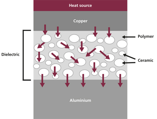
The red arrows represent the heat. The white circles are thermally conductive particles within the dielectric that transport the heat to the aluminium layer.
The dielectric serves as medium for the thermal conduction, but also for insulation purposes as well as for bonding copper and aluminium. The thermally conductive dielectric is available with ceramic filler that may either be woven-glass reinforced or unreinforced. Aluminium substrates are generally preferred due to their better machinability. Alternatively, substrates including copper or steel can be used.
Choice of the appropriate IMS subtrate
Choice of the appropriate IMS subtrate
In order to chose the appropriate IMS substrate for the respective application, the properties listed in the following charts should be considered..
1. Dielectric
| Dielectric with wovenglass reinforcement | Dielectric without wovenglass reinforcement | |
|---|---|---|
| Breakdown voltage | high | lower |
| Cost | low | high |
| Breakdown voltage | lower | higher |
| Thickness uniformity | better | worse |
2. Effect of Filler on thermal Conductivity and Breakdown Voltage
| Filler type | Thermal conductivity (W/mK) | Breakdown voltage based on 70% filler |
|---|---|---|
| Al2O3 | 25~40 | + + |
| MgO | 25~40 | + |
| SiO2 | 9.6 | + |
| Si3N4 | 50 | - |
| BeO | 270 | - |
| SiC | 25~100 | - - |
| AlN | 120~220 | + |
| BN | 100~250 | + |
++ excellent, + good, - bad, - - poor
Typical Characteristics of IMS Substrates
Typical Characteristics of IMS Substrates
| Thickness | Thermal conductivity (W/mK) | |
|---|---|---|
| Copper | 18 µm - 410 µm 1) | 380 |
| Aluminium | 0.5 mm - 3 mm | 200 |
| Dielektrikum | 75 µm - 150 µm | 0.4 - 0.8 / up to 2.5 2) |
| Fr4 | 0.4 |
1) Copper thicknesses, 2) woven-glass reinforced dielectric
What exactly is thermal Conductivity W/mK?
Thermal conductivity may not be confused with thermal diffusivity, i.e. the speed with which a change in temperature diffuses within a medium. Thermal conductivity exclusively refers to the heat conduction and not to the heat transfer by convection or thermal radiation. The heat conductance coefficient in Watt per Kelvin (W/K) is an index depending on the dimensions of a module. The thermal conductivity of materials is measured pursuant ISO22007-2 by means of the HOT-disk-method.
Should you have any questions regarding the ISO standards, please do not hesitate to contact us
When selecting a material for an application, the thermal impedance has to be taken into consideration as well. The thermal resistance (Rth) defines the interior thermal resistance of a material against a possible heat flow. The lower this value, the better the heat can be dissipated through the material. Thermal impedance is comparably characteristic as Rth, yet strictly referring to the constant of the contact surface.
If the breakthrough voltage is no decisive factor in the choice of the material, it frequently makes sense to chose a thinner dielectric and a lower thermal conductivity. Thus, it is possible to reach nearly the same thermal impedance (see chart).
By rule of thumb: The lower the W/mK value of the basic material, the lower is its price.
Thermal Impedance for different Values of thermal Conductivity
| Dielectric | W/mK = 1.6 | W/mk = 2.2 |
|---|---|---|
| 75 µm | 0.074 | 0.054 |
| 100 µm | 0.074 | 0.054 |
| 125 µm | 0.074 | 0.089 |
| 150 µm | 0.148 | 0.107 |
For most LED applications, materials with lower W/mK values are perfectly adequate.
CTE-Differences within IMS Materials
CTE-Differences within IMS Materials
- Materials ppm/°C
- Aluminium:24
- Epoxy:85
- Glass fabric:6
- Cooper:17
CTE Values for the individual IMS Materials with varying W/mK Values
CTE Values for the individual IMS Materials with varying W/mK Values
| Material e.g. Ventec: | VT-4A1 | VT42 | VT4B3 |
|---|---|---|---|
| W/mk: | 1.0 | 2.0 | 3.0 |
| Dielektrikum: | with glass | with glass | without glass |
| CTE values (ppm/°C) | |||
| x,y: | 13 | 12 | 21 |
| before Tg (z axis): | 32 | 25 | 44 |
| after Tg (z axis): | 150 | 140 | 198 |
| Total (z axis): | 2.00 % | 1.80 % | 2.70 % |
IMS materials are offered with Tg values ranging between 90 °C and 170 °C.
In case of different lighting applications, the breakdown voltage is not decisive for the functional safety due to the fact that the operating voltage is relatively low. In this context, it is much more important that the individual modules are exposed to severe thermal cycling due to the seasonal ambient temperatures and humidity variations.
The CTE differences between copper, dielectric, aluminium and ceramic components result in shear stresses. At worst, these stresses and strains may cause fatigue cracks at the solder joints or in ceramic components and the de-lamination of the laminate. The use of glass reinforced dielectrics reduces the CTE mismatch between the substrate and the ceramic components and consequently also the default rate.
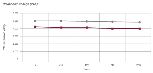
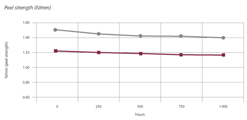
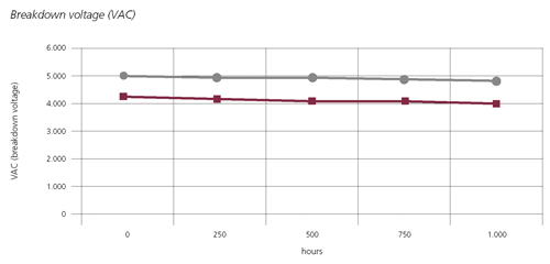
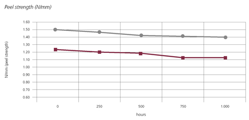
Effects of thermal Cycling on Breakdown Voltage and Peel Strength
Effects of thermal Cycling on Breakdown Voltage and Peel Strength
- Test blanks:
- 1.50 mm aluminium / 100 µm dielectric / 35 µm copper with 1 W/mK and 2 W/mK
- Test conditions:
- -50 °C (30 min.) – 150 °C (30 min.) 500 cycles
- Test materials:
- VT-4A1 + VT-4A2
Source: Ventec Electronics
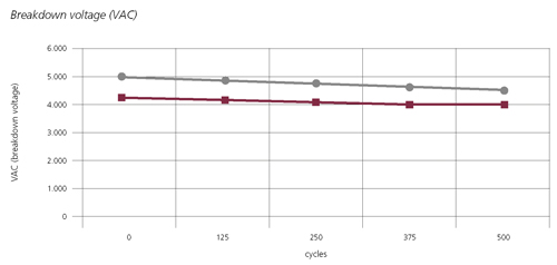
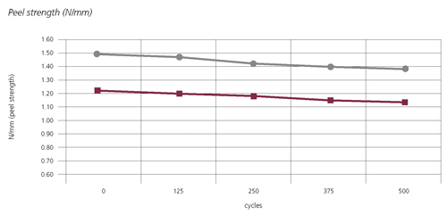


In test series over 500 cycles, there are only minimal further changes in both values.